
The wait-state generator was created to insert one or two extra clock cycles in a 65C02 or 65C816 system. This could be
used to interface slower memories or IO devices in a system with a fast system clock.
This device takes advantage of the RDY pin in the microporcessor. When this pin is pulled low, the microprocessor will freeze until it goes high again. If done during PHI2's high pulse, the CPU address and data bus values will be held stable. This stretches the CPU cycle to allow slower devices to respond.
One feature of this device is that it can be programmed to insert either 1 or 2 wait states based upon a built-in memory address decoder. Fast RAM will have 0 wait-states, slow ROM will have 1, and a slower IO device will have 2 wait-states. This will all be controlled automatically.
Here is a schematic of the logic - WS1 and WS2 are generated by the address decoder:
The memory adddress decoder can be programmed for any configuration desired. For an example, here is how the default source is written for a GAL16V8 20-pin DIP package:
Slow ROM at address $C000-$CFFF
Slow IO at address $D000-$DFFF
Slower IO at address $E000-$EFFF
Slower ROM at address $F000-$FFFF
To see the results in action, I am including a capture of the WinCUPL Simulator program:
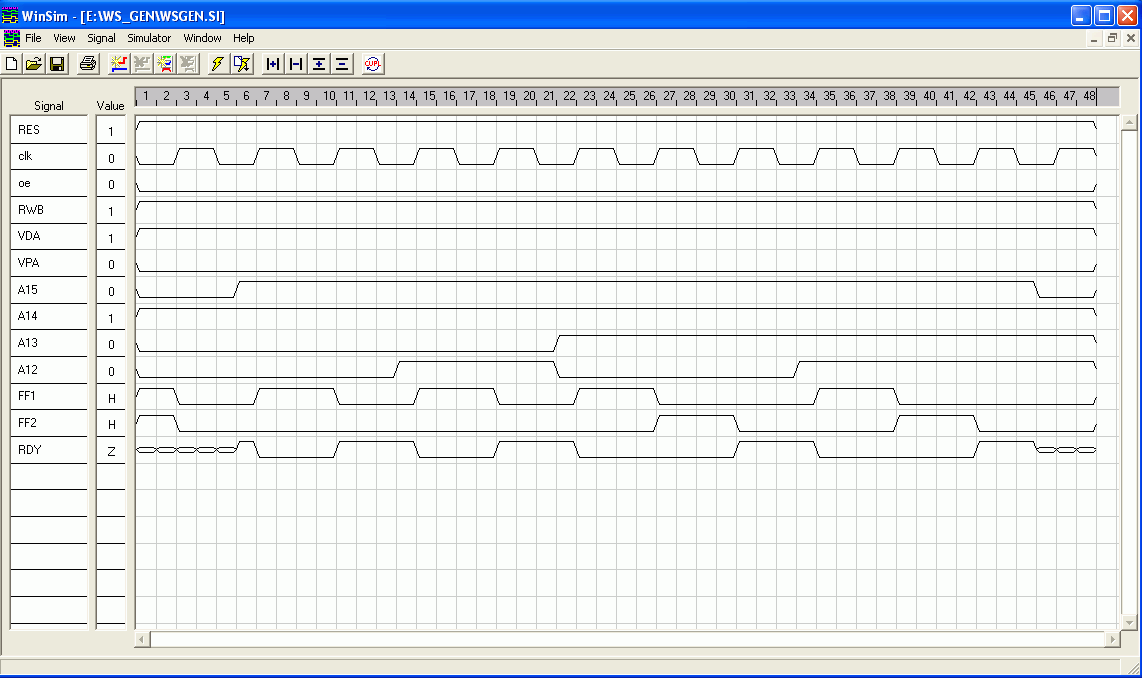
For this example, focus on the clk (PHI2), A15-A12, and RDY
The PHI2 clock cycles from column 5 - 12 are for ROM addressed in the Cxxx range and provide 1 wait state.
The PHI2 clock cycles from column 13 - 20 are for IO addressed in the Dxxx range and provide 1 wait state.
The PHI2 clock cycles from column 21 - 32 are for IO addressed in the Exxx range and provide 2 wait states.
The PHI2 clock cycles from column 33 - 44 are for ROM addressed in the Fxxx range and provide 2 wait states.
One option included here is that RDY is tristated when the address decoder determines no wait state is needed. This, and many other options could be deisgned into this device.
The source for this device looks like this:
                         /*             __   __              */
Name     WaitStateGen;   /*   PHI2 -> 1|  |_|  |20<- VCC     */
PartNo   1;              /*    VDA -> 2|       |19-<>        */
Date     12/04/2010;     /*    VPA -> 3|       |18-<>        */
Revision 01;             /*    RWB -> 4|       |17-<>        */
Designer Daryl Rictor;   /*    A15 -> 5|       |16-> ws2     */
Company  ;               /*    A14 -> 6|       |15-> ws1     */
Assembly ;               /*    A13 -> 7|       |14-> RDY     */
Location ;               /*    A12 -> 8|       |13-> FF2     */
Device   g16v8ms;        /*   /RES -> 9|       |12-> FF1     */
Format   j;              /*    GND ->10|_______|11<- GND     */

/*********************************************************************************/
/*                                                                               */
/*  This program and its associated documentation are provided for your personal */
/*  use only and appear here exclusively by permission of the copyright holder.  */
/*  Please contact the copyright holder before re-distributing, re-publishing    */
/*  or disseminating this copyrighted work. This code is not GPL or in the       */
/*  public domain. Please respect the author's copyright.                        */
/*                                                                               */
/*  No waranty, either expressed or implied, are given.  I assume no liability   */
/*  for its use in any project or device.                                        */
/*                                                                               */
/*  Your use of this program indicates your acceptance of all license terms.     */
/*  This particular version is freeware as long as the copyright messages are    */
/*  left intact.                                                                 */
/*                                                                               */
/*********************************************************************************/

/* INPUTS  */

pin 1     = clk;                        /* FF clock input */
pin 11    = oe;                         /* FF Output Enable */

pin 2     = VDA;                        /* MPU valid data address */
pin 3     = VPA;                        /* MPU valid program address */
pin 4     = RWB;                        /* MPU read/write */
pin 5     = A15;                        /* address bus */
pin 6     = A14;                        /* address bus */
pin 7     = A13;                        /* address bus */
pin 8     = A12;                        /* address bus */
pin 9     = RES;                        /* system /RES input */

/* OUTPUTS */

pin 12    = FF1;                        /* Flip-Flop 1 */
pin 13    = FF2;                        /* Flip-Flop 2 */
pin 14    = RDY;                        /* MPU RDY signal */
pin 15    = ws1;
pin 16    = ws2;


/* LOGIC */

Cxxx      = A15 & A14 & !A13 & !A12 & (VDA # VPA) & RWB;     /* Cxxx = ROM 1 ws */
Dxxx      = A15 & A14 & !A13 &  A12 & (VDA # VPA);           /* Dxxx = IO 1 ws */
Exxx      = A15 & A14 &  A13 & !A12 & (VDA # VPA);           /* Exxx = IO 2 ws */
Fxxx      = A15 & A14 &  A13 &  A12 & (VDA # VPA) & RWB;     /* Fxxx = ROM 2 ws */

/* Combinatorial OUTPUTS */

ws2       = Exxx # Fxxx;                /* OR all logic elements that require 2 wait states */
ws1       = ws2 # Cxxx # Dxxx;          /* OR ws2 with all logic elements that require 1 wait state */
RDY.oe    = ws1 ;                       /* tri-state RDY when not needed */
RDY       = !FF1 & !FF2;                /* condition MPU RDY input */

/* Register OUTPUTS */

FF1.d = (ws1 # ws2) & !FF1 & !FF2 & RES;   /* FF1 holds wait state #1 */
FF2.d = ws2 & !FF2 & FF1 & RES;            /* FF2 holds wait state #2 */

/* End */
The source and compiled JED file can be downloaded here -> wsgen.zip
| Home |